← AC Capacitor Wiring Diagram: The Ultimate Guide for DIY Enthusiasts wiring diagram for ac capacitor compressor Why Are Schematic Wiring Diagrams Important to Technicians? Simplify Repairs! Understanding wiring diagrams for eaton electrical systems →
If you are searching about How to Use a Modular Approach to Simplify Your PCB Design Process you've visit to the right web. We have 25 Images about How to Use a Modular Approach to Simplify Your PCB Design Process like Pads Schematic Tutorial Pads Schematic Suite Es Capture, Pads Layout Viewer Download: The Key to Streamlining Your PCB Design and also 22 steps to summarize the entire PCB design process - IBE Electronics. Read more:
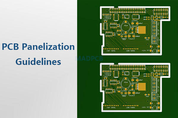
How To Use A Modular Approach To Simplify Your PCB Design Process
 www.linkedin.com
How to Use a Modular Approach to Simplify Your PCB Design Process
PCBWay's KiCad Plugin: Simplify Your PCB Design Process - Semiconductor
 www.semiconductorforu.com
PCBWay's KiCad Plugin: Simplify Your PCB Design Process - Semiconductor ...
Basic Pcb Design Software
 circuitdbunerupted.z21.web.core.windows.net
Basic Pcb Design Software
Via-in-Pad Design | PCB Knowledge - YouTube
 www.youtube.com
Via-in-Pad Design | PCB Knowledge - YouTube
PCB
 www.slideshare.net
PCB
Pads Schematic Tutorial Pads Schematic Suite Es Capture
 diagramaduttnx5.z21.web.core.windows.net
Pads Schematic Tutorial Pads Schematic Suite Es Capture
PCAD PCB Design: The Ultimate Guide For Beginners – Hillman Curtis
 hillmancurtis.com
PCAD PCB Design: The Ultimate Guide for Beginners – Hillman Curtis ...
Simplify PCB Design With Interactive Routing - YouTube
 www.youtube.com
Simplify PCB design with interactive routing - YouTube
Pads Schematic Tutorial Pads Schematic Suite Es Capture
 diagramaduttnx5.z21.web.core.windows.net
Pads Schematic Tutorial Pads Schematic Suite Es Capture
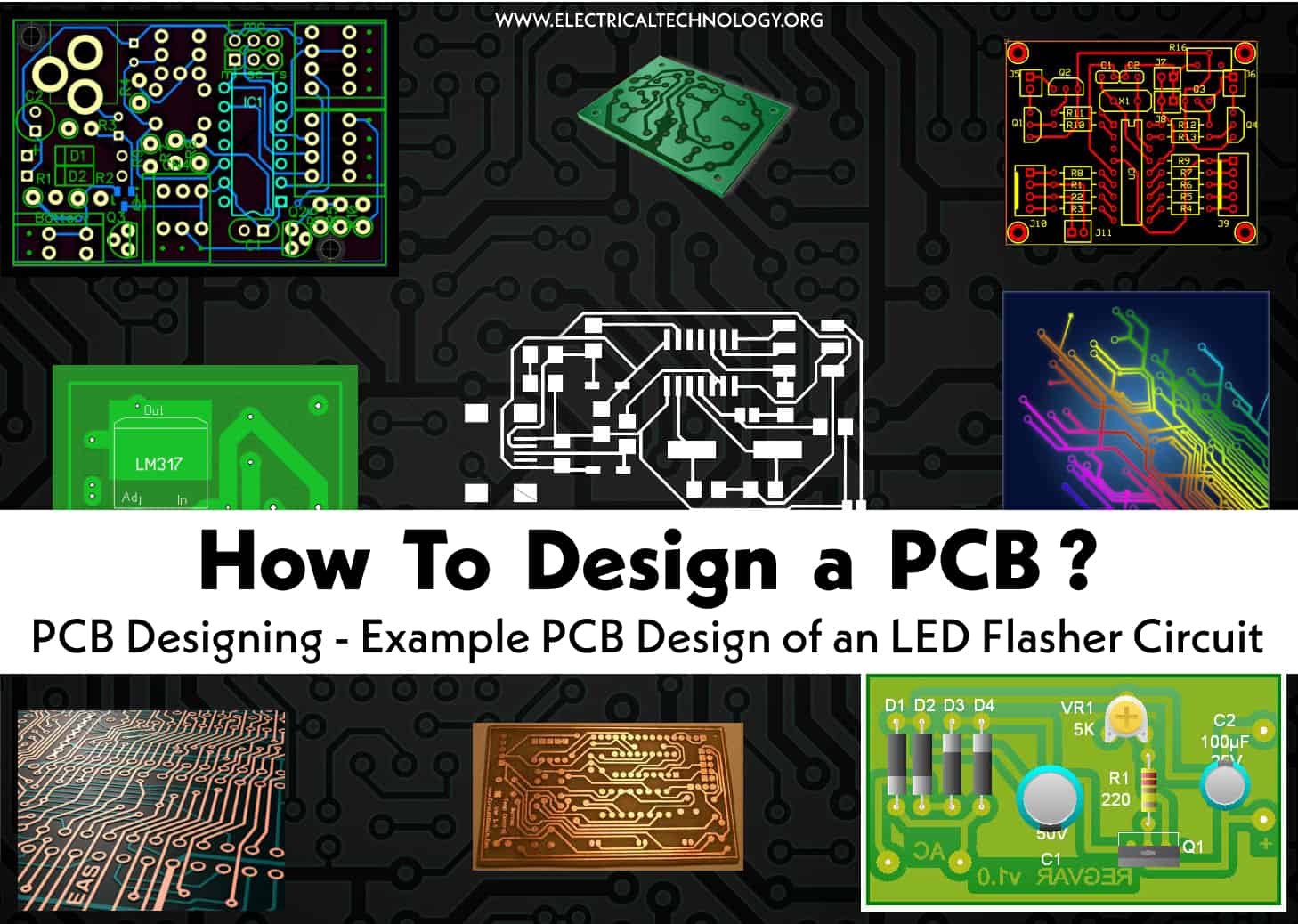
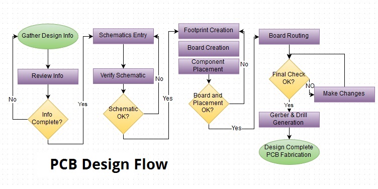
The Processes Of PCB Design That You Should Know
 how2electronics.com
The processes of PCB Design that you should know
A Step-by-Step Guide On How To Use PADS Layout
 hillmancurtis.com
A Step-by-Step Guide on How to Use PADS Layout
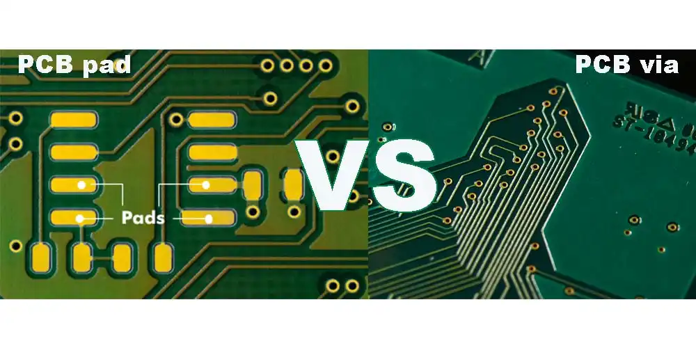
PCB Pad – A Basic Guide For Beginners - Mainpcba One-stop PCB Assembly
 www.mainpcba.com
PCB pad – a basic guide for beginners - Mainpcba One-stop PCB Assembly ...
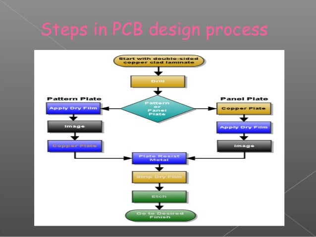
PCB Design Process
 mungfali.com
PCB Design Process
Pcb Design Steps - Design Talk
 design.udlvirtual.edu.pe
Pcb Design Steps - Design Talk
Pads Schematic Tutorial Pads Schematic Suite Es Capture
 plewaltesyrer1f9guide.z14.web.core.windows.net
Pads Schematic Tutorial Pads Schematic Suite Es Capture
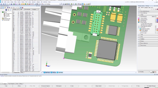
SOLIDWORKS PCB Software For PCB Schematics & Mechatronic Design
 www.javelin-tech.com
SOLIDWORKS PCB Software for PCB Schematics & Mechatronic Design
The Complete Guide To PCB Pad :types, Size, Spacing, Repair And
 qtech-us.com
The complete guide to PCB pad :types, size, spacing, repair and ...
22 Steps To Summarize The Entire PCB Design Process - IBE Electronics
 www.pcbaaa.com
22 steps to summarize the entire PCB design process - IBE Electronics
Pads Layout Viewer Download: The Key To Streamlining Your PCB Design
 www.raypcb.com
Pads Layout Viewer Download: The Key to Streamlining Your PCB Design ...
Basic Steps To Design A PCB Layout | Quadcept Help Center
 support.quadcept.com
Basic Steps to Design a PCB Layout | Quadcept Help Center
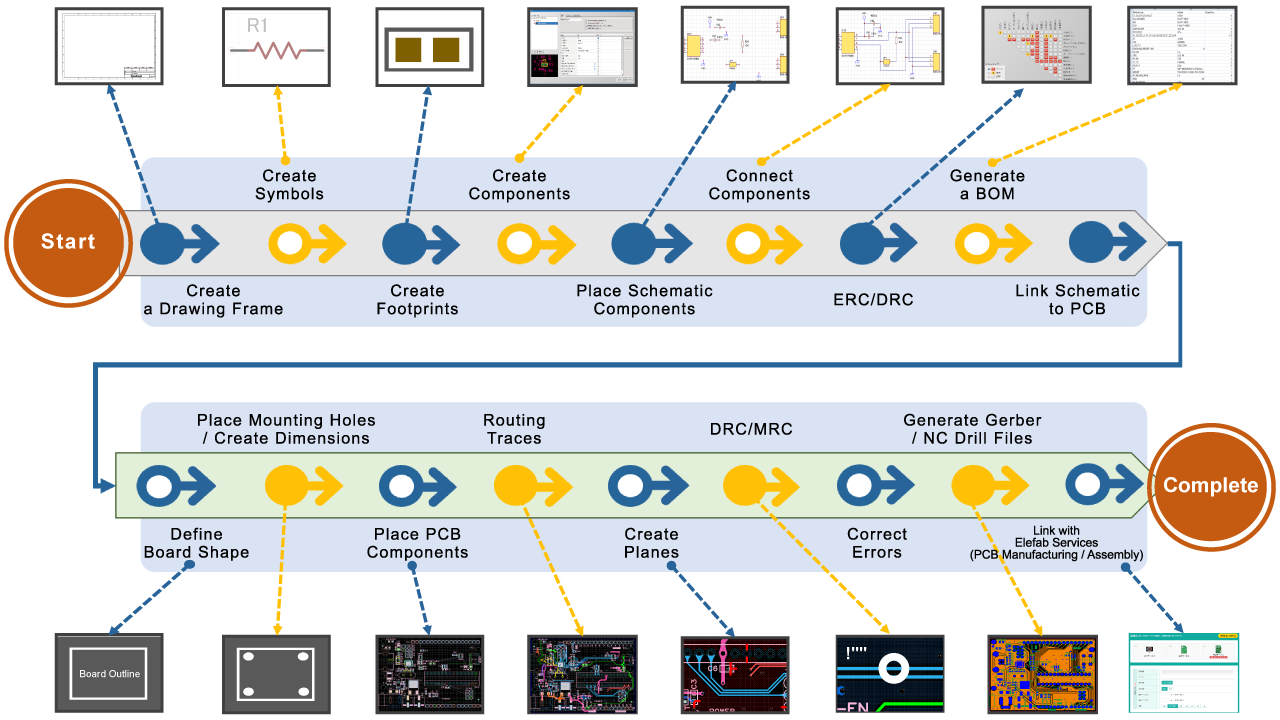
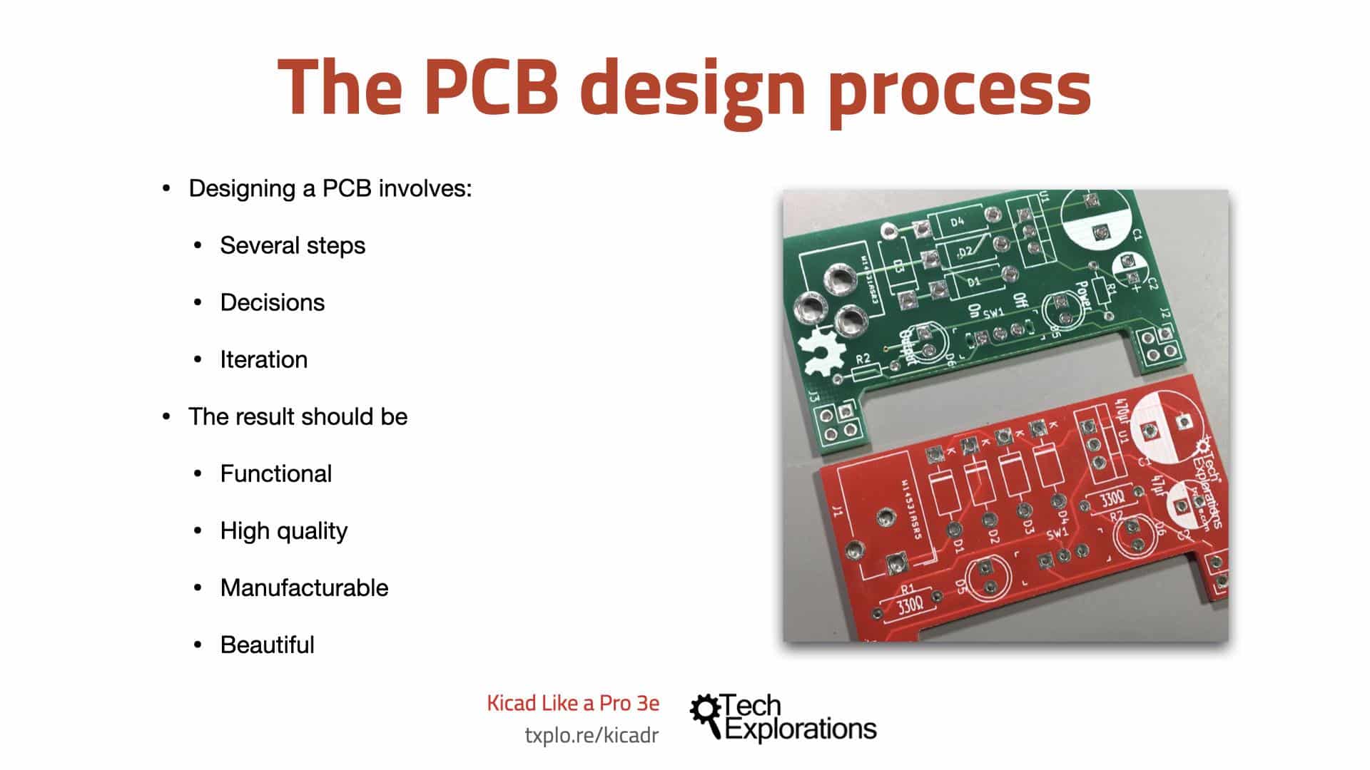
Tech Explorations - KiCad 6 Guide Series - The PCB Design Process
 techexplorations.com
Tech Explorations - KiCad 6 Guide Series - The PCB design process
Pads Layout Viewer Download: The Key To Streamlining Your PCB Design
 www.raypcb.com
Pads Layout Viewer Download: The Key to Streamlining Your PCB Design ...
PCB Process Flow Chart | Www.homillux.com
 www.homillux.com
PCB Process Flow Chart | www.homillux.com
PADS Professional: The All-in-one Design Suite | PADS Desktop PCB Design
 blogs.sw.siemens.com
PADS Professional: the all-in-one design suite | PADS Desktop PCB Design
A Guide To Pcb Design Process Aipcba - Vrogue.co
 www.vrogue.co
A Guide To Pcb Design Process Aipcba - vrogue.co
The processes of pcb design that you should know. Basic steps to design a pcb layout. Solidworks pcb software for pcb schematics & mechatronic design